Formation of a CMOS Transistor
- saumil vora

- Aug 26, 2020
- 4 min read
Greetings Readers!
In this blog, the fabrication process of the CMOS transistor will be discussed in detail. In the previous blog in the CMOS basics category, the formation of PN junction was discussed with an example of how electron-hole pairs conduct the current (click here to read). Keeping the concept of p-type and n-type semiconductor material in mind, let us build a CMOS inverter to understand the fabrication process of the CMOS circuits.
Importance of Understanding the COMS Fabrication Process
Being a physical design engineer, we have to deal with the base layers' rules provided by the foundry. These base layers are nothing but the layers involved in the fabrication of a transistor. Physical design is the last stage before we give the chip for fabrication. Thus, it is the responsibility of a PD engineer to meet all the foundry rules requirement and make the chip manufacturable. This can be achieved only when we are familiar with the chip fabrication process, which layers are involved in the fabrication of the device, and which technology we are working on.
With this, hope the readers are convinced why it is necessary for the backend engineers to understand the CMOS fabrication process.
Formation of the CMOS Transistor
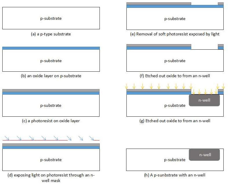
A CMOS transistor consists of both, a PMOS and an NMOS transistor. That is why it is called Complementary MOS transistor (CMOS). Mostly, a CMOS transistor is built on a p-type base of a silicon wafer which is known as p-type substrate. The first step is to create an n-well inside the p-type substrate. This is done by injecting pentavalent impurities into a part of the p-type substrate. To develop an n-well, a thin protective layer of oxide is formed on the p-substrate. Then we remove the oxide layer from the area where we want to grow the n-well. A photoresist is used in this process of removal. Then pentavalent dopants are injected on the entire substrate but it will penetrate only in the region where the oxide layer is removed. The process of forming an n-well is shown in figure 1.

The photoresist becomes soft when exposed to the light. An n-well mask is used to soften the photoresist only in a particular area. In other regions, it remains hard. The soft photoresist is removed and the oxide layer in that region is also etched out.
The next stage is to form the transistor gate. The gate is generally formed of the polysilicon material. First, a thin oxide layer is formed on p-substrate inside a furnace. Then the polysilicon layer is grown inside a reactor using the process called Chemical Vapor Deposition. As we have seen in the process of n-well formation, here also photoresist and gate mask is used for the formation of the transistor gate. Polysilicon gates are heavily doped to make it a good conductor. In recent times, polysilicon gates are used instead of the metal gates reasons being:
Polysilicon is a semiconductor and thus conductivity can be controlled by controlling the doping amount.
The polysilicon gate can offer a lower threshold value than that of the metal gate because the work function difference between a poly gate and the channel is very less.
The next step is to create the diffusion regions in both, NMOS and PMOS. Two n+ regions are created in the p-type region and one n+ well contact is created in the n-well region. These regions are created using the ion implantation method. Only the area where regions have to be created are exposed to dopants while all other region is covered with an oxide layer. Here poly gate of the NMOS acts as a blockage for the ion implantation in that region hence n+ regions are automatically separated without any mask. This space between the source and drain regions acts as the channel. In a similar manner, p+ diffusion regions are formed inside the n-well and a p+ contact is created in the p-substrate region. The formation process of the gate, n+, and p+ regions are also highlighted in figure 2.

This is the basic fabrication process of a transistor. Once the transistor is fabricated, metal layers are laid off on top of it. With technology advancement, the channel length is shrinking. This channel length is the deciding factor for the technology node. For instance, a 14nm technology node means the channel length between the source and the drain region is 14nm.
The major challenge in device size shrinking is that it cannot go below the wavelength of the light used in the photolithography process. Apart from this many second-order effects also come into the picture as channel length reduces. Another major challenge with technology advancement is that metal widths are getting shrunk which reduces their current carrying capability and increases the RC-delay. Also, the number of metal layers is increasing. For example, a 14nm technology node can have 8 metal layers while 7nm technology node can have up to 15 metal layers. In that also, the first three to four metal layers have double patterning. Which means there are two masks for each of these layers. This is required because the pitch of the below few metal layers is so less that during the etching process these layers may get short-circuited with each other. To overcome this issue two masks are used for the same metal layer. For instance, if METAL1 is having double patterning (i.e. two masks) then all the nets of METAL1 having the mask-1 will be laid off first then the other nets of METAL1 having the mask-2 are laid off. This increases the fabrication complexity and DRC rules for sign-off checks also.
Basic fabrication processes and the effects of technology advancement are explained in this blog. Second-order effects of MOS transistors will be covered in a separate blog as it requires a detailed explanation. Hope readers find this blog useful and please share your feedback or other queries in the comment section below.
To read other blogs on physical design concepts click on the below links.

Comments