
Importance of Semiconducting Materials in VLSI
- saumil vora

- Jul 31, 2020
- 7 min read
Updated: Sep 30, 2020
In high school, we have studied that depending upon the electrical property, all materials can be divided into three categories namely conductors, insulators, and semiconductors. Out of these materials, semiconductors have got much importance in chip fabrication. This blog will discuss why semiconductors are highly preferred in the VLSI industry, types of semiconductors, and what happens when we combine two types (n-type and p-type) of semiconducting materials. In the end, will discuss how these concepts relate to MOS transistors.
Understanding the Importance of Semiconductors
Why semiconductors are chosen over conductors when we can have a higher current carrying capability in conductors? A very obvious question, right? Let us find the answer to this question in this section. Let us understand the importance of semiconductors over conductors or insulators from their atomic structure and energy bandgap. These terms might remind you of your school days!
As we all know that conductors are the materials that can conduct electric current very easily, on the other hand, insulators do not conduct electric current, and semiconductors can conduct a moderate amount of current. Let us understand the difference between a copper atom (conductor) and a silicon atom (semiconductor). Figure 1 shows the atomic structures of both, copper and silicon.
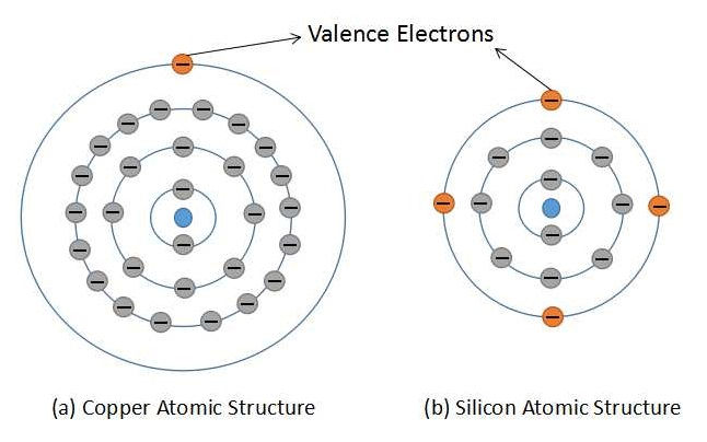
The copper atom has 29 protons and 28 electrons (excluding valence electron). This makes a net charge of +1 for the copper atom. For silicon, there are 14 protons and 10 electrons (excluding valence electrons) which makes a net charge of +4 for silicon atom. Another major difference in both the atomic structures is that the copper atom has a valence electron in the fourth orbit while silicon has valence electrons in the third orbit. With both the above points we can conclude that the valence electron in copper can very easily leave its orbit and can become a free electron. While for the silicon atom we need to apply a little more energy to convert valance electrons into free electrons. From the above discussion, we can derive a point that conductors can conduct current with very little energy applied from outside. This property makes conductors undesirable for designing IC components as the device can turn on even without applying external voltage. Only room temperature will suffice to turn on the device. With this, devices made up of conductors can exhibit a higher leakage current. The third type of material is an insulator, in which a very high amount of energy has to be applied from outside in order to conduct current in the device. Thus to use insulators is not a feasible idea. Let us understand this concept using the energy band diagram as shown in figure 2.
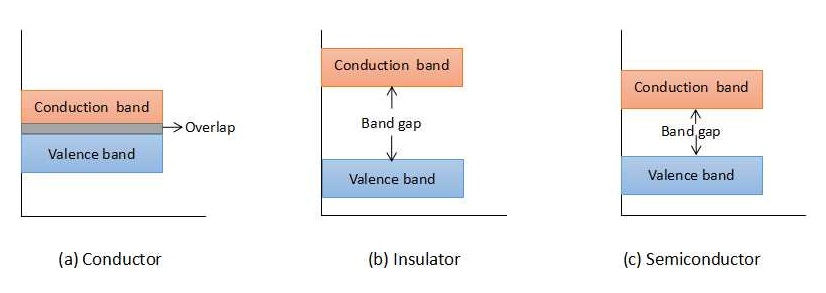
The valence band represents the energy level of the valence electrons (electron in the outermost orbit of an atom). When a valence electron gets sufficient energy to leave its orbit, it becomes a free electron that can conduct the current in the device. This energy level is represented by the conduction band. The valence and conduction band overlap each other in conductors, in insulators, they are very far, and in semiconductors, they are at a moderate distance. Thus, a different amount of energy is required for electrons to jump from the valence band to the conduction band in all these devices. Here also semiconductor comes out to be a clear winner.
Another major factor is that semiconducting materials can share their valence electrons by forming a covalent bond. This gives chemical and electrical stability in the intrinsic semiconductors. Conducting materials cannot form a covalent bond to achieve stability. With all these points, the semiconducting material is highly preferred over conductors and insulators in the VLSI industry. It is so popular that our entire industry is also known as the Semiconductor Industry.
Types of Semiconductors
Semiconductors can conduct only a limited amount of current in its intrinsic (pure) form. The reason being they contain very few free electrons (or holes) that can take part in current conduction. The conductivity of semiconductors can be controlled by adding impurities to the intrinsic semiconducting material. This process of adding impurities is called doping. Based upon the impurities added and the majority charge carrier in the device, we can categorize semiconducting material in two groups namely n-type and p-type semiconductors.
1. N-type Semiconductor:
An N-type semiconductor can be obtained by doping the intrinsic semiconductor with pentavalent atoms. The atoms which have five valence electrons are called pentavalent atoms, for example, Arsenic (As), Bismuth (Bi), Antimony (Sb), and Phosphorus (P). In an intrinsic silicon atom, each valence electron forms a covalent bond with four neighboring atoms. Instead of a silicon atom if we have one pentavalent atom such as Arsenic (As) then one extra electron will be available as a free electron. Both of these examples are shown in figure 3. Pentavalent atoms are known as donor atom as they donate one extra electron for current conduction.
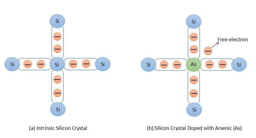
In pentavalently doped silicon atom, electrons are in the majority which contains negative charge. Hence, a semiconductor doped with the pentavalent atom is known as an n-type semiconductor. In an n-type semiconductor, when an electron jumps to the conduction band from the valence band it leaves behind a void space which is termed as a hole. A hole is nothing but the absence of an electron. Thus, holes are also present in an n-type semiconductor but they are very few, known as minority charge carriers.
2. P-type Semiconductor:
A p-type semiconductor can be obtained by doping the intrinsic semiconductor with trivalent atoms. The atoms which have three valence electrons are called trivalent atoms, for example, Boron (B), Gallium (Ga), and Indium (In). In an intrinsic silicon atom, each valence electron forms a covalent bond with four neighboring atoms. Instead of a silicon atom if we have one trivalent atom such as Boron (B), having three valence electrons, creates one void space which can be filled by an electron. Both of these examples are shown in figure 4. One electron can jump into the hole leaving a space behind. In this manner, the hole moves in the direction opposite to that of an electron. Trivalent atoms are known as acceptor atom as they can accept one extra electron for current conduction.
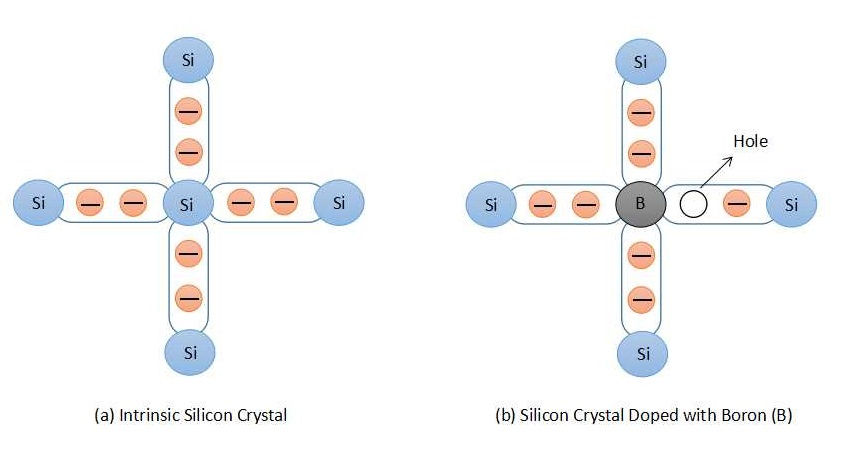
Majority charge carriers in the p-type semiconductor are holes and electrons are minority charge carriers.
The above discussed are the two types of semiconductors that can be formed by choosing the appropriate doping atom. The number of charge carriers can be controlled by the amount of doping. This topic forms the foundation for the NMOS and PMOS structures which we will discuss in upcoming posts.
Forming a PN Junction
When we dope a part of a piece of silicon with trivalent impurity and another part with the pentavalent impurity then a PN-junction is formed, as can be seen from part (a) of figure 5. In the p-type region, the majority charge carriers are holes while in the n-type region it is electrons. Both the sides few minority charge carriers are also shown which are generated due to thermally excited charge carriers on the respective sides.
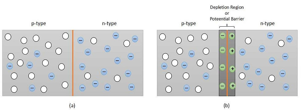
Now, free electrons at the n-region are attracted by the holes in the p-region. This forces few electrons (in the n-type region) closer to the boundary of both the regions to jump across the p-type region. This creates a positive ion in the n-type region from where an electron has jumped. Similarly, holes are attracted to the n-type region and leave behind a negative ion in the p-type region. This phenomenon gives rise to the depletion region or the potential barrier. It is shown in part (b) of figure 5. The depletion region expands till both the regions become electrically neutral.
Once the depletion region is created it repels charges at both the sides at stops them from crossing the junction. Now if we want this device to conduct the current then we need to apply external energy in the form of potential difference (voltage) equivalent to the potential difference of the depletion region. This potential is known as barrier potential. The barrier potential is measured in the form of voltage (V). The barrier potential value depends upon the material used and the operating temperature. For instance, the barrier potential. at 25 degrees Celcius, for Silicon is 0.7V and for Germanium it is 0.3V. This is one of the reasons why silicon is preferred over germanium in the industry and this makes germanium leakier than silicon. Other reasons being silicon is easily available in the form of sand and in a huge quantity, silicon crystal can withstand higher temperature than that of the germanium crystal. One major advantage of germanium is that electron and hole mobility is higher in it as compared to silicon. Thus, germanium can offer a higher speed than silicon.
How These Relate to MOS Transistors?
All the above theories we have studied in school or college. The purpose to discuss them again in the form of a blog is to form a strong foundation for understanding the operation of a MOS transistor which will be covered separately in other posts. From the basics of the transistor, we all know that a transistor is also made up of PN-junctions. In the case of BJT transistors, PNP or NPN junctions are formed. If we talk about MOSFET, NMOS transistor is formed by creating n-type terminals (source and drain) on a p-type silicon layer whereas a PMOS transistor is formed by creating p-type terminals (source and drain) on n-type silicon layer.
When we will discuss the current conduction in MOS transistors, it will become easy to understand if we have knowledge of how current conduction takes place in PN-junction.
Hope you are now clear with the fact that why semiconductors are so widely used in the VLSI industry. Please feel free to share your views with me.
Below are the links to my other blogs.
Please subscribe to this blogging site to stay updated with the latest blogs.
Stay Safe, Stay Happy... :)
Comments