
Clock Tree Synthesis - Part 1 : Introduction to the Clock and the CTS Terminologies
- saumil vora

- Jul 7, 2020
- 5 min read
Updated: Jul 10, 2020
Since the establishment of the first IC, semiconductor industry has been constantly evolving. Today, multiple complex functionalities can be implemented on a single chip. Along with this advancement, high performance requirement is also increasing rapidly. Some leading IC manufacturers have developed processors that can operate at more than 2GHz frequency. After few years this may also be seemed as low frequency. Incorporating millions of cells inside a chip operating at such a high speed needs very accurate and strategically planned clock network.
Clock network plays very pivotal role in achieving timing and power requirements. It is believed that up to 40% of total power is consumed by clock network itself. This can further rise with increasing clock frequency. A balanced clock network helps in achieving timing goals without much difficulty. Thus, Clock Tree Synthesis (CTS) turns out to be very significant stage in physical design flow.
This blog provides information about concepts related to CTS as listed below. These are the concepts one need to understand before implementing the clock tree.
The Clock Signal
Goal of CTS
Prerequisites for CTS
CTS specification file
CTS Exceptions
Inputs and outputs of CTS
The Clock Signal
Digital VLSI systems are build using the synchronous design approach. In this design style millions of transistor operates at a regular interval of time. This switching activity of the gates is controlled using the Clock signal. A design can have a single or multiple clock based upon requirement. Before going to CTS, let us first understand few important terms related to the clock.
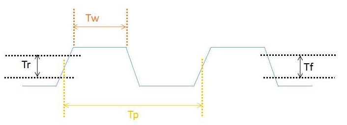
Rise Time (Tr) : Time taken by the clock signal to rise from 10% to 90% (or 20% to 80% in some cases) of the maximum value is known as clock rise time.
Fall Time (Tf) : Time taken by clock to fall from 90% to 10% (or 80% to 20% in some cases) of the maximum value is known as fall time.
Time Period (Tp) or Clock Period : Clock period is defined as the time period between two active edges of the clock. Active edge can be either rising edge or the falling edge based upon the type of flip-flop to which clock is fed. In figure 1, rising clock edge is considered as the active edge.
Pulse Width (Tw) : Pulse width is defined by the time period for which clock cycle remains in active state.
Duty Cycle : Duty cycle is the ratio of on-time of the clock cycle to the total clock period. In ideal case, duty cycle should be 50% i.e. clock period is divided equally between on-time and off-time of the clock. Duty cycle can be calculated using below equation:

Note : In order to achieve the better timing results, rise time (Tr) and fall time (Tf) of the clock should be same. That is why special buffers and inverters are used to build clock tree which has equal rise time and fall time.
Goal of Clock Tree Synthesis
Major objective of CTS stage is:
To propagate clock to every sequential element in the design
To achieve skew and latency targets
To optimise setup and hold timing
To meet CTS design rule constraints such as max transition, max capacitance, etc.
To attain optimised clock power
Prerequisites for CTS
Before beginning the CTS stage, it is advisable to perform certain sanity checks so that clock tree can be build accurately. Below is the checklist to follow.
Design is placed and optimised.
Setup timing and congestion should be under control.
Check the clock source definitions in SDC file.
Check the CTS specifications (skew, latency, NDRs, etc.) defined in CTS spec file.
Check for all the tool settings related to CTS implementation and optimisation.
Remove don't use attributes from clock cells.
If any pre-placed clock cells are required make sure they are placed at proper location and should be fixed.
PG nets should be routed.
High fanout nets should be synthesised.
Check the active scenarios for CTS.
Clock Tree Specification File
All the specifications required to build a clock tree are kept in a file called clock tree spec file. This file is written in TCL format with tool specific commands. Information inside the CTS spec file is as below:
Clock naming convention
Skew and latency targets
Design rules related to transition, capacitance, fanout, etc.
List of clock buffers and inverters to be used in CTS
Non-Default Rules (NDR) for clock routing
Min and max routing layers for clock tree
It can be concluded that building of clock tree can be controlled using CTS spec file. We can change the parameters defined in CTS spec file as per requirement.
Clock Tree Exceptions
PnR tools automatically derives the clock source point (clock root) from create_clock statement defined in the SDC file. Then tool traces through the clock fanout network and derives clock endpoints too. Basically there are two types of end points that tool can recognise, these are:
Sink pins which are the clock endpoints. Endpoints which can be considered as sink pins are clock pin of a register that should not drive a generated clock, clock pin of a macro, clock root, output ports, non-clock pin of a sequential cell. Tool considers sink pins for delay balancing (skew and latency optimisation) and to fix design rules (tran, can , and fanout).
Ignore pins are those pins on or beyond which tool does not perform delay balancing but can perform design rule fixes.
Sometimes designer need to specify endpoints other than default derived by the tool. These user-defined endpoints are termed as clock tree exceptions. Few clock tree exceptions are:
Through pins are pins at which delay balancing is not performed but beyond this pin tool can perform delay balancing. For example, clock pin of a flip-flop driving a generated clock or an ICG cell. Through pins are also known as non-stop pin.

Float pin is a pin at which special insertion delay is applied in order to meet the skew target. An example of float pin is shown in figure 3. Here insertion delay for FF1 is 100ps so to keep the same insertion delay for FF0 we need to specify an insertion delay of 80ps at the SRAM pin. In this scenario macro pin becomes float pin as delay balancing is considered w.r.t clock pin of FF0 instead of SRAM pin.

Exclude pin is a clock tree endpoint which is completely excluded from delay balancing by tool. Timing optimisation is also not performed on this pin. Tool performs only design rule checks at this pin. It is similar to the ignore pins derived by tool the only difference is exclude pins are explicitly defined as ignore pins by designer. Examples of exclude pin is same as that of ignore pins described above.
Stop pin has attribute same as the sink pins derived by tool automatically the only difference is stop pins are defined explicitly by the designer.

Input and Output of CTS
The input files required for CTS are:
Placement DEF and netlist files
SDC file for timing constraints and clock definition
LIB and LEF libraries
CTS specification file
RC extraction file to estimate wire delay
Don't use and don't touch cells' list
You can read about few important input file here. In order to analyse the CTS results, below reports should be generated after CTS implementation:
Skew and latency reports
Setup and hold timing reports
Design Rule Verification (DRV) report (transition, capacitance, fanout, long net, etc.)
Design Rule Check (DRC) report to analyse shorts, opens, or metal DRCs related to clock network.
Power consumption report
Design utilisation and congestion report
I will restrict this blog up to here only. CTS itself is a very huge topic as it requires a lot of concepts to learn so that one can build an accurate clock tree. Next topic I am going to cover is clock skew, latency, and uncertainty followed by the implementation and analysis of the clock tree. Please feel free to bring up any query related to topics covered in this post. Meanwhile stay happy, stay safe...!! :)


Comments