
Floorplanning - Significance, Strategies, Computations
- saumil vora

- Jun 17, 2020
- 7 min read
Updated: Jul 24, 2020
Greetings Readers !!! :)
It is very well known fact in VLSI industry that a good floorplan can save lot of time and energy of design engineer. One might think why floorplanning is so important? What are the strategies to achieve a good floorplan? How to proceed for floorplan and to check whether floorplan is accurate or not? All these question will be answered in this post. Topics covered in this blog are as follows:
Importance and goal of floorplanning
Floorplan styles
Floorplan stages
Calculation for die area
Inputs and outputs of floorplanning stage
I hope people find this post informative and interesting. Let's dive deep into floorplanning...
Importance and Goal of Floorplanning:
"A good beginning is a half battle won", this proverb very well fits for floorplanning stage in the physical design flow as well. A good floorplan improves both the productivity of subsequent physical design steps (placement, CTS, etc.) and the time of the design cycle. This is why enough time should be given for creating an accurate floorplan and with experience one can create accurate floorplan in less number of iterations.
The primary goal of floorplan is to place hard macros in the core region with sufficient area available for standard cells and routing. An accurate floorplan leads tool to place cells closer to each other (based upon hierarchy and connectivity) and hence helps in achieving timing closure, lower routing congestion, and reduced IR drop.
Floorplan styles:
There are two styles in which macros can be placed which gives us two floorplan types namely: abutted floorplan and channelled floorplan.
Abutted Floorplan:
In this floorplan style, macros are placed adjoining to each other without leaving any space in between. Generally this style is not recommended because channel is required in between macros to serve purpose for routing, buffering of macro pins and to meet implant layer spacing rules.
Figure 1 shows an example of abutted floorplan. In this figure macros U1, U2, U3, and U4 belongs to same hierarchy whereas U5 and U6 lies in different hierarchy hence shown by different colours. Here it can be clearly seen that there is no space available for routing and buffering the macro pins. In lower technology nodes this can also violate implant (n-well, p-well, vt layer, etc.) layers spacing rules.

Channelled Floorplan:
Channelled floorplan is one in which appropriate spacing is provided between macros. Minimum spacing between macros can be computed using below formula:

For example if there are 100 pins in a macro on layer M3 whose pitch is 0.5 microns. In total we have 8 metal layers available for routing out of which 4 are vertical layers and 4 are horizontal. According to above formula, minimum vertical spacing = (100*0.5)/(4) = 12.5 microns.
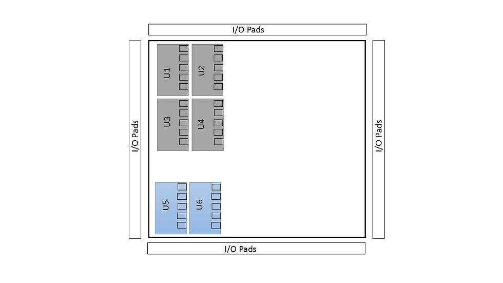
Figure 2 represents an example of a channelled floorplan. Here vertical spacing between all the macros is clearly visible. Purpose of keeping vertical channel between macros are listed below:
To route macro pins
To buffer macro pins in order to fix timing or DRV issues
To ensure at least one power and one ground stripe passes through channel
To meet implant layers min spacing rules
One can also see a horizontal channel between macros U1-U3 and U2-U4. There is no specific formula to calculate horizontal channel but one can decide it based upon number of I/O ports placed near to that region. Standard practice is to decide horizontal channel based upon congestion report.
Apart from these two floorplan styles one can also use abutted and channelled mixed floorplan style. One must need to understand design requirements very clearly before opting for mixed floorplan style.
Floorplan Stages:
Broadly speaking floorplanning comprises of 3 major stages.
Macro placement
Port placement
Power planning
Now we will discuss these 3 stages in detail.
i. Macro Placement :
This stage comprises of placing the macros in the core region such that enough area is available for standard cell placement and routing. There are various factors which should be taken care of while placing the macros, few major factors are listed below.
Place the macros across the edge of block. By doing so sufficient area is left for standard cell placement. The metal layers which are used for connecting logic inside macro are blocked for routing over the macros. Thus by placing a macro in the centre of block will create congestion. Refer Figure 3 below.
The macros belonging to same hierarchy should be placed closer to each other. This is to avoid module splitting and to make optimum use of routing resources. In Figure 3 macros are highlighted by different colours to indicate different hierarchies.
Provide adequate channel between macros for routing and buffering of macro pins.
Place macros in such a manner that all its pins are facing towards the core region. By doing so, congestion and route length from macro pins to its fanout logic can be reduced.
Provide hard placement blockage/halo across all the edges of all macros. Purpose of doing so is to ensure that standard cells are not placed in macro channel otherwise it will increase channel congestion. Only buffers/inverters are allowed to place in macro channel. In some cases, complex IPs need minimum separation from logic cells this also can be achieved by using halo. In Figure 3 halos are shown in red box across the macros.
Macro orientation is also an important factor to consider while placing it. If pins in a macro are aligned vertically (as in all macros in figure 3) then place macro in vertical position only. Anyways horizontal orientation for this macro is not allowed reason being it will change the orientation of all metal layers used inside macro and also there will be chances of short connection among the pins. Allowable orientation for all any macro can be found either from it's properties or from CELL LEF file.
Place macros having more height near to the edge of the block and macros having lesser height next to it. As represented by macros U7 and U8 in Figure 3.
There are certain technology specific requirements as well which designer should take care while floorplanning.

ii. Port Placement :
Port placement refers to the placing of I/O pads across the block edges. In some cases location of ports will be provided by partitioning team. This will be based upon the requirement of chip top level. If there is any communication between ports and macros then in that case place the ports first as per top level requirement then after place the macros. If there is no specific requirement from top level then one need to identify the ports belonging to same logic and place those ports close to each other. It is standard practice to place ports in a manner that its routing is not blocked by macros. If this is not possible then keep sufficient spacing between ports and macros for routing and anchor buffers (buffers for I/O ports).
If feedthrough ports are available make sure they are not placed in criss-cross manner otherwise it can increase routing congestion. To control the congestion near ports it is required to spread ports with some distance apart. Nets used for clock ports will require non-default rules (NDR) so for this reason also one need to provide adequate spacing between ports.
iii. Power planning :
Primary goal of power planning is:
To decide number of PG pins required
To decide the width of power ring and power stripes
To decide the number of power stripes
To maintain minimum possible IR drop across the block
Creation of voltage are/power domain if required
In general power routing is given highest priority over clock and signal routing. Reason being power routing is highly critical and occupies a lot of routing resources in design. To reduce the IR drop, most of the power routing is done on higher metal layers. Higher the metal layer more is the layer width which reduces the resistivity of metal routes. Power planning can be done manually or can be done automatically with the help of tool. Few basic formulas used in power planning are as follows:

Current density of metal layer in above equations can be obtained from Tech LEF file. In the equation of PG stripe width, current on each side is multiplied by 2 because we have to consider current flowing from two opposite sides of the block. Power routing is done using 3 elements which are Pads, Ring, and Stripes. Figure 4 represents a typical structure of power planning.

Power pads are used to draw power inside the chip. From pads power transfers to power rings. A PG ring is created across the block. Power is supplied inside block using horizontal and vertical power stripes.
Apart from creating power mesh, creation of voltage area is also an important task during power planning. One can get information regarding multiple power domains from UPF file. Based upon that create voltage area corresponding to each power domain described in UPF file. Size and shape of voltage area can be decided based upon number of logic cells present in that particular power domain. Also ensure other power gating cells such as level shifter, power switch, isolation register, etc. are defined in UPF file.

Calculation for Die Area :
To start floorplanning one may need to calculate the actual die area required to implement entire logic in core area. Total die area and standard cell row area can be calculated using below formula:
Die area = (Total std. cell area + Total macro area)/0.7
In above equation, std. cell area and macro area should constitute around 70% of total die area. Around 30% of area is left empty as buffers and inverters will be added during optimization and hold timing fixing. That is why in above total equation std. cell area and macro area is divided by 0.7. It is not mandatory to keep 30% of free space, one can keep it 25%, 20%, or 35% based upon design requirement. Total row area available for standard cell placement can be computed using formula:
Placeable row area = Die area - macro area - hard placement blockage area
Another important parameter to decide floorplan is Aspect Ratio of the block. Aspect ratio can be computed as:
Aspect Ratio = Block width/Block height
Aspect ratio of 1 means it is a square block, greater than 1 means block height is more than its width and vice-versa if aspect ratio is less than 1. Aspect ratio plays a vital role as it decides weather to stack macros vertically or horizontally. Also more height means more amount of horizontal routing resources are available as compared to vertical routing resources. More width means more vertical routing resources are available as compared to horizontal resources.
Inputs and Outputs for Floorplanning :
Various input files required to kick start floorplanning are:
Synthesized netlist (.v)
Technology LEF and CELL LEF
Timing library (.lib)
Design constraints (SDC)
Unified Power Format (UPF)
RC delay file
Block level DEF file (optional)
Port location file (optional)
Macro location file (optional)
For detail insight about types of input files in physical design flow, one can refer here.
Output files after performing floorplanning are:
Floorplan DEF(.def)
Floorplan netlist (.v)
Initial utilization report
All macros and ports are placed
Creation of voltage area if required (.va file)
I have tried to accumulate all the important points which are required to achieve an accurate floorplan. It is very difficult to get an exact floorplan in single shot, it requires multiple iterations. With more experience one can become more familiar with floorplan strategies and can achieve goal in lesser amount of time. Please feel free to reach out for any further discussion. Hope you might have enjoyed reading this blog. Will be coming soon with another informative post till then STAY HAPPY, STAY SAFE....! :)


Well explained all things
well explanation saumil
Hi Damarla,
In most of the cases, macro pins will be placed in vertical position. Horizontal macros are very rare. Since pins are vertically placed, we need to calculate the horizontal spacing (or vertical channel) between the macros for pins to route properly. This is not the case with the vertical spacing (or horizontal channel), so we do not use any specific formula for the horizontal channel between macros. Regarding core power and voltage that we can get from the UPF or any other power-related input file.
Hi Very good explanation.
I have a doubt why don't we calculate the horizontal spacing b/w macros using the same formula?
In the formula, you mentioned macro pins is 100 that means these 100pins are in vertical direction side?
In power-planning, how/from where we get total core power and core voltage?
Thank you Shwetha.