
Physical Design Flow
- saumil vora

- May 24, 2020
- 4 min read
Updated: May 25, 2020
Greetings Readers!!!
To kick start with physical design, it is always a good practice to begin with the flow. This blog will provide a brief idea about different stages involved in physical design cycle. So let's dive into the world of physical design!
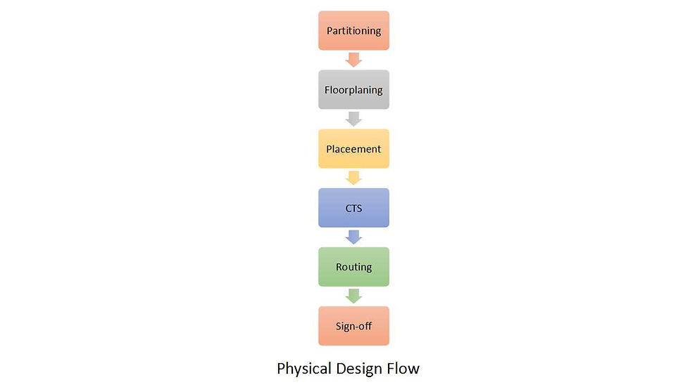
Partitioning:
VLSI domain has experienced a rapid growth in terms of technology nodes. This growth is mainly based on the Moore's Law which states that number of transistors packed inside an IC is getting double at almost every 24 months.
Today technology has grown to an extent where we can pack millions of transistors in a chip sizing few mm square.
In such condition it becomes very complex to handle entire chip by single person/team.
In order to reduce the complexity of design handling, run time, and time to market, it is utmost necessary to break down entire chip into smaller blocks. This is known as partitioning of a chip.
Few points to be taken care while partitioning:
Original functionality of the design should remain same
Partitioning process should be time efficient
Minimum possible interface between partitioned blocks
Hierarchy of design should be considered while partitioning
Decide the number and location of ports in each block
2. Floorplanning:
Broadly speaking, floorplanning involves 3 stages:
Place macros (SRAMS, IPs, Analog blocks) in core region
Macros should be place in such a manner that enough area is available for placing standard cells without causing huge congestion.
Various factors to be considered while placing macros will be discussing in upcoming blogs.
Pin assignment
Once macros are placed, ports should be placed at the edges of block.
In some cases, ports location will be provided by chip top team, if not then one can place ports based upon macro placement i.e. ports and macro in same hierarchy to be placed near to each other.
Power planning
Main goal of power planning stage is to provide regular power in entire core region with minimum possible voltage drop.
In this stage, width and pitch of power/ground stripes has to be fixed.
In case of multi-voltage or power shut-off design, voltage area has to be created at this stage itself. This information one can get from UPF file.
Physical only cells such as end-cap cells and tap cells will be placed at this stage.
3. Placement:
Main goal of placement stage is to provide legal position to all the standard cells in core area.
A good placement can save area, routing resources and power dissipation in design.
Accuracy of the placement can be decided from congestion and timing reports.
If congestion and setup timing are within specified limits then only it would be good to go for CTS stage otherwise need to review floorplan and placement stages.
4. CTS:
Almost every VLSI system is synchronous in nature. Which means at least one clock is required to control the data flow in design.
The process of planning and implementing the clock tree structure is called Clock Tree Synthesis (CTS) .
Prime objective of CTS is to place clock cells and route clock network to achieve skew and latency targets.
A good quality of CTS can help saving clock power and reduce timing violations in design.
CTS itself is a very vast topic which cannot be covered in single blog. There will be series of blogs on CTS to have complete insight on it.
5. Routing:
Once all the targets till CTS stage are achieved, now design comes into final stage of PnR (Place and Route) flow which is routing.
Routing is basically being carried out right from floorplan till CTS.
At floorplan stage we will perform routing of power and ground nets. During placement, coarse routing will be performed to calculate setup time. During CTS stage clock nets will be routed in the design.
After giving priority to power and clock nets, at this stage we will perform accurate routing of signal nets.
Routing is done in two stages i.e. Global routing and Detail routing.
Target of routing stage is to completely route the design without any net open and/or short. Also DRC (Design Rule Check) count should be under control.
Timing after detail route should be feasible.
All the above factors will conclude whether the recipe used in PnR flow has worked out or not. If results are not satisfied then multiple iterations can be performed starting from floorplan upto routing stage with different parameters.
6. Sign-off:
Once all the desired targets in PnR and ECO stage is achieved, various checks need to be performed on the design before taping out the chip.
These series of checks are collectively known as sign-off checks.
Objective of performing sign-off checks is to improve the yield and to ensure hassle free performance of IC after fabrication.
Sign-off checks includes:
Functionality verification (LEC- Logic Equivalence Check)
Max tran, max cap, high fanout, min pulse, glitch checks
Timing checks (it is recommended that design is timing clean before tape-out )
Signal Integrity (SI) checks
EM (Electro-Migration) and IR (voltage drop) checks
Physical verification (DRC, ERC, LVS checks)
This blog is intended to provide a brief understanding of PD flow. In forthcoming blogs, will be discussing in detail about each stage introduced above. Hope you might have enjoyed reading this post. Next blog will be coming soon till then Be Happy, Be Safe and Keep Learning!!! :)


Comments