
Placement - Part I
- saumil vora

- Jun 25, 2020
- 10 min read
Updated: Jul 6, 2020
Greetings Readers!! :)
"Better the Placement, easier to achieve the PPA (Power-Performance-Area) targets", agree? Once we are done with floorplanning, next stage in Physical Design flow is Placement. The behaviour of placement is highly dependent upon the floorplan stage thus it is very much important to have a proper floorplan before we proceed for placement. Placement itself is a huge topic so will be publishing it in two parts. In first part topics covered are as listed below.
Importance of placement
Prerequisites for placement
Pre-placement stage
Placement stage
Scan chain reordering
Possible issues after placement
Inputs and outputs for placement stage
While in second part will be discussing briefly about different types of cells, and significance of bounds, blockages, and keepout margins in placement.
After reading this post, readers will be able to answer important questions related to placement such as what is the significance of placement? What are the steps required to consider before commencing placement? How to perform placement? How to improve placement QoR (Quality of Result)? What are the files required to start placement? and What are the outcome of placement? Let's place the design then...
Importance of Placement :
Primary goal of placement stage is to provide legal position to all the logic cells, used in design, within the core region. By legal position it means each and every cell should have unique position in core region, cells should be placed exactly within row and should not overlap any other cell or macro in the design.
Placement stage has significant impact on each of the PPA (Power, Performance, and Area) parameter. A good placement can save a lot of area, routing resources, IR drop, and can reduce RC delay. Thus we can say that placement lays the foundation stone to achieve desired PPA targets.
Prerequisites for placement :
Before starting placement, there are certain checks which needs to be passed in order to get good placement QoR (Quality of Result). These checks are:
Floorplan should be completely done according to floorplan guidelines. Make sure that floorplan DEF and .v files are available to kick start with placement.
All the macros or any other pre-place cells (if present in the design) should be marked as locked so that they are not displaced during placement optimization.
Make sure that all the ports are properly placed, power planning is done as per requirement, and voltage areas are created if multiple power domain exists in the design.
Check pre-timing of the design. This is the setup timing check before starting placement in order to confirm that the design which we have received from the synthesis team does not have timing violations or if violations exists then it should be minimal.
Macro channel congestion should be either zero or minimal.
For lower technology nodes, if there exists any base DRC related to macro placement then give the highest priority to fix it. Ignoring base DRCs at this stage can increase the turnaround time.
Look out for any error or critical warning in floorplan log file. If exists then make out a plan to resolve it.
Verify the list of don't touch and don't use cells.
Check the consistency of libraries and constraints.
Check for the applications options and other settings done in the tool to achieve desired PPA targets.
Pre Placement Stage :
Before placing the standard cells, there are certain other cells which needs to be placed. These cells serve some special purpose and their position needs to be fixed once placed hence they should be placed first. These cells are:
Endcap cells
Tap cells
Decap cells
Spare cells
Apart from these there can be power gating cells or clock gating cells which needs to be pre-placed based upon design requirements.
Apart from pre-place cells, designer needs to create bounds and/or blockages if there is any requirement as per guidelines from chip-top level. After first iteration of placement, one can create additional bounds or blockages based upon congestion and timing reports. If there exists complex cells like AOI/OAI cells which tends to have higher pin density then provide appropriate keepout margin or padding for these cells. This will help to control pin density and congestion in design. The detailed description on various types of cells, bounds, blockages, and keepout margin will provide in next blog on placement.
Along with this, designer need to apply settings for placement optimisation in order to achieve desired PPA targets. Sometimes design can be congestion critical or timing critical or both, accordingly choose the settings in PnR tool. In some cases criticality of the design cannot be determined at first iteration itself for such cases perform placement with default settings then in second iteration choose your recipe based upon the outcome of first iteration.
Placement Stage :
After placing pre-placed cells, creating bounds/blockages/padding, and after choosing proper settings for the design, now we are good to go for placement stage. There are 3 stages involved in placement, which are:
Global placement, Legalization, and Placement optimisation (Detail placement)
i. Global/Coarse Placement :
Global placement simply places all the logic cells within the core area with cells distributed evenly across the block. At this stage factors like placing the logic cells within standard cell rows, cell overlapping and routability of nets are not considered. A rough placement is created which forms the base for legalization and placement optimisation.
ii. Legalization :
Prior to optimise design for placement, it is necessary that all the logic cells have a unique legal position in the block and cells should be placed with allowed orientation within the rows. Major role of legalization is to remove overlap of cells and place cells within standard cell rows with minimum possible displacement of cells from its original position set at global placement stage. Before going for optimisation, one must make sure that legalization process is completed without any error otherwise optimisation will not happen properly.
iii. Placement Optimisation :
Placement optimisation is performed on successfully legalized design. Objective of the placement optimisation can be as follows:
To place cells within same hierarchy close to each other i.e. not to split hierarchical module
To achieve even cell density and pin density across the block
To improve routability of the design or reduced congestion in other words
To achieve better timing (mostly setup timing) results by placing cells connected to each other as closer as possible
To achieve transition, capacitance and fanout targets
In order to achieve optimisation goals, global routing is performed during placement stage. This helps to get an estimation of congestion and timing. In order to achieve the desired targets, following three tasks are performed during placement optimisation stage.
Removing buffer trees
Sizing and displacement of movable objects
Adding buffers or inverter pairs
To summarise we can say that placement is performed in order to place all the logic cells at a legal position in the block considering the settings provided in PnR tool and other constraints like bounds, blockages, or keepout margin in order to achieve desired PPA targets.
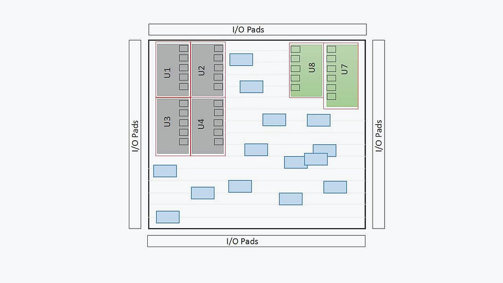
The concepts of global placement, legalization and placement optimisation (detail placement) can be understood from images shown below. Figure 1 shows an illustration of the outcome of global placement. Here one can observe how cells are placed in random manner. Whereas figure 2 shows an example of how outcome of legalization and placement optimisation would look. In figure 2 number of cells are shown more because of buffer/inverter pair insertion during opimisation stage.

Scan Chain Reordering :
Scan chain is inserted into the design in order to test the continuity and accessibility of each node in the design. Scan chain is nothing but a series of D flip-flops connected together. It begins from the scan input port, traces through all the flip-flops in scan path, and terminates at scan output port. This arrangement helps in testing the data flow in chip at any point of time. An example of scan chain is shown in figure 3.

During placement stage these flops gets displaced from their position in order to place standard cells appropriately. As a result, connection if flip-flops becomes criss-crossed which can increase congestion in the design. Scan chain after placement optimisation will be as shown in figure 4.

As it can be observed from figure 4 that register FF1 is displaced from its position and due to that routing length has increased. Here comes the need to reorder the scan chain. In above case of we connect register FF0 to FF2, register FF2 to FF1, and FF1 to FF3 then route length for scan flops can be reduced which helps in controlling cngestion. Refer to figure 5 for connection of flip-flops after scan chain reordering.

Possible Issues After Placement :
Major issues which one can observe after placement are:
High congestion/ high cell density or pin density
Poor setup timing
Legality issues
More IR drop
It is not necessary that all the time these issues will be seen. Some designs can see all reports clean in first iteration itself. Such situations happens very rarely though. Whereas in few cases some of the above mentioned issues may arise. This totally depends on criticality of the design. You might be wondering how to fix if any of these issues encountered after placement? Let us discuss them one-by-one.
i. High Congestion/Cell density after Placement :
If you find more congestion in macro channel then it's a floorplan issue. To fix this one need to provide more channel between macros or even try out by changing the macro positions. This can also occur if hard placement blockage is not provided in the channel area and cells are placed in channel during placement. In worst case, if there is no space to give in macro channel and no other floorplan is helping out to reduce congestion, one can put a request to increase the block size to top level. But before that enough experiments should have been done to justify the area increment.
One may also see congestion in the core region. To fix this there are many ways. First of all check that hierarchy is not getting split-up. If you found module is splitting then definitively congestion figure will jump up. If tool is not able to place cells in the same module near to each other then try to create bound for such modules. This will place cells in a module in that bound and can help in controlling congestion. It is considered as a good practice to keep bound utilisation in between 50%-55% in first iteration. Based upon the output of first iteration, designer can alter bound utilisation according to congestion in or around the bound.
Another way to fix congestion issue is to create partial placement blockage in the region where congestion is higher. By creating partial placement blockage we ask tool to adjust the cell density in that particular area. A partial blockage with 30% blocked area means it will allow only 70% cell density in that area. It is also termed as density screen. One can also create density screen in entire core area to control cell density and congestion.
One can also choose appropriate cell density settings available in PnR tool. Designer can also turn on the options related to congestion aware placement and increase the effort of optimisation stage to reduce congestion.
ii. Poor Setup Timing :
Setup timing will be calculated once placement is completed. Tool will perform global routing in order to incorporate RC delay of the nets. Most importantly clock is ideal during placement stage. Thus clock uncertainty will be provided to the tool to incorporate clock path related propagation delays. One needs to observe WNS (Worst Negative Slack), TNS (Total Negative Slack), and Number of violating paths in placement timing report. If you observe that too may paths are violating or WNS and TNS are very high then it is very important to fix these timing issues. There are multiple ways to fix timing issues, few are listed below.
First of all if there is any module splitting then fix it.
Check the bufferability of nets. Sometimes tool is not able to buffer a particular net due to multiple reasons.
Group the violating paths together increase it's priority and weightage to fix timing during optimisation.
Fix max tran, and max cap related issues.
Create buffer tree for high fanout nets.
By increasing the clock uncertainty value during placement optimisation will help in fixing timing violation. By doing so we are tightening the optimisation constraint for tool. Make sure to keep clock uncertainty to original value while generating the timing report.
There can be various other techniques to fix timing based upon design requirement. Most important is to observe the timing report and cells placement in the block. Using these information one can plan out the fixes for timing violation.
iii. Legality issues :
Sometimes tool is not able to find a legal position for the cell as design can be highly congested, cell type is not matching with the row type, cell belongs to other power domain, or the cell type used in not allowed. If any cell is failing legalization then tool will fail to perform optimisation in such cells and one can see too many violations in the design.
To avoid legality failure make sure that don't use cell list is defined and it contains all the cell names which are not allowed in the design. If design is too congested then first fix the congestion and cell density issues. Also make sure that cell's PG pins are properly connected to respective PG nets in the design. If tool is not able to resolve overlap over few cells then designer can do it manually is enough space is available nearby.
iv. IR Drop issues :
If too many cell density is higher at a particular region inside the block then it can lead to more IR drop. So try to spread cells in such area. If there are complex cells like multi-bit flops, AOI/OAI cells which has more number of pins then apply cell padding or keepout margin for such cells. These are power hungry cells. Also check for route length, too long nets tend to have more IR drop.
One can also use density screen to spread cells in order to reduce IR drop. Sometimes if too many macros are clustered together then it can also lead to more IR drop. For such scenario try to give some spacing between macros. If nothing works out then need to re-consider on power planning i.e. either increase the width of PG stripes or decrease the PG pitch.In some cases logical restructure might be required to reduce IR drop. This need to be informed to designer team and they will do necessary changes in design.
Inputs and outputs for placement stage :
Input files required to start placement are:
Floorplan DEF and netlist (.v)
LEF and LIB files
SDC file
UPF file (in case of low power or multi voltage design)
Don't touch and don't use cell list
RC delay file
Some important files and reports which should be generated on completion of placement are:
Placement DEF and netlist
Utilisation report
Congestion report
Timing report
In this blog I have tried to cover basic concepts of placement. Hope you find this blog informative. There will be one more blog on placement in which I will discuss about various types of cells used in PD flow, bounds, blockages, and padding (keepout margin). Once again feel free to provide you feedback. See you soon, till then Stay Happy, stay safe...!! :)


thanks for sharing