
An Introduction to Static Timing Analysis
- saumil vora

- Jul 27, 2020
- 4 min read
Updated: Jul 31, 2020
Greetings Readers !!!
"Time and Tide Waits for None" a well-known quote that we have heard many times. This quote is equally applicable to Static Timing Analysis as well (only for the time parameter, not the tide). With this blog, I am starting a series of posts on STA. I hope you will enjoy the journey.
In this introductory blog, an attempt is made to cover three important questions viz. Why timing analysis is required? What is STA?, and How to perform STA?. Learning these three concepts will help the designer to build a strong foundation to carry out timing analysis accurately. Also, it will be helpful for readers to learn the in-depth concepts of STA, which will be coming soon, easily. In the end, will discuss about input and output for the STA tool. So let us plunge into the world of STA.
Purpose of Doing Timing Analysis
Almost all the VLSI designs are synchronous. It means, at least one clock is required to perform operations in sync. If data transfer is not in sync with the clock then it may lead to failure of the chip. This condition makes it necessary to analyze the timing in design.
Today, millions of logic cells get implemented in a single chip. Each cell in the design must undergo timing analysis. One approach for this can be to apply input vectors to the gates and check its functionality w.r.t the clock. In this scenario, the timing simulation of the chip will be an exhaustive process. It may take up to years to perform timing simulation of the entire design. It makes input vector based timing analysis practically impossible. Then what should be done to perform timing analysis? How can we make sure that the chip will not fail due to timing issues? The answer to the above questions is Static Timing Analysis.
What is Static Timing Analysis
In STA, we perform timing analysis without providing any input vectors to the design, so it is called "static". It does analysis based on the logical functionality of the cells. In this way, STA provides us a faster and more accurate approach to carry-out timing analysis. In this approach, the aim is to validate whether the design will operate at a given frequency or not. If the analysis report comes out to be positive then we can ensure that chip is ready to operate at the given frequency.
Few checks carried out in STA are setup and hold timing checks, recovery and removal timing checks, signal integrity checks (cross talk and noise), DRV checks (tran, cap, etc.). These checks are performed for all possible logic paths and at various environmental conditions (PVT scenarios). This makes STA an exhaustive process to verify the performance of the design.
How STA is performed?
Consider a logic path under analysis as shown in figure 1. To calculate the setup timing, the tool will calculate delays as mentioned below.
Delay of register U/FF0. This delay is the time taken for the flip-flop to produce the data at pin Q after receiving an active clock edge at the CK pin. This is called CK to Q delay of the flop.
Cell delay for U/AND1 gate. This delay is the time taken by the signal to travel from U/AND1/A to U/AND1/Z. In a similar way cell delay for U/BUFF1 is calculated.
Then tool adds the setup time of flip-flop U/FF1 (which is obtained from the lib file) to the above delay.
Along with the cell delay, STA also incorporates the wire delay also known as RC delay. At sub-micron technology nodes, RC delay plays a very significant role in timing analysis.
Adding up all the delays mentioned above makes up arrival time for this particular path.
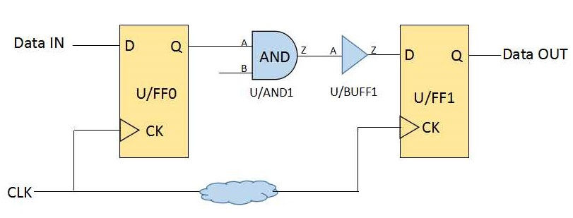
For hold time analysis, delays will be considered as mentioned below.
CK to q delay for U/FF0
Cell delay for U/AND1 and U/BUFF1
RC network delay
Summation of all the above delays should be greater than the hold time of flip-flop U/FF1
The above two are very basic examples of how STA calculates delay for setup and hold timing analysis. In the above examples, min & max delays, rise & fall time of signals, and PVT conditions are not considered for simplicity. Timing analysis with all those effects will be discussed in upcoming blogs on STA.
Inputs and Outputs of STA
Major input files required to start the STA run are:
Netlist of the routed design
RC delay and cell delay file (SDF file, liberty file)
SDC file
The output of the STA run will be:
Setup and hold timing reports
Timing QoR reports
DRV reports such as max tran, mac cap, fanout load, min clock pulse, clock double switching, etc.
To summaries, performing STA on routed design ensures the designer that the chip will function properly at the given frequency. The purpose of writing this blog is to introduce the concept of STA to the readers who are new to the VLSI domain. Slowly we will dive deeper into the world of STA covering all important topics. Stay tuned for more blogs on STA.
Other Blogs
To read blogs on all the stages of Place and Route flow, click the below link.
To know more about the different types of files required in PD, click the below link.
Note: To stay updated with the latest blogs, readers can subscribe to the mailing list by submitting your mail address at the end of the page.


Comments