
Setup and Hold Time - Part 2: Analysing the Timing Reports
- saumil vora

- Aug 13, 2020
- 6 min read
Updated: Aug 14, 2020
Greetings Readers!
In the previous blog, setup and hold time concepts were discussed in detail (click here to read). Now, this blog is mainly based on analyzing the setup and hold timing reports generated by the STA tool. For timing analysis, paths can be categorized into four categories mentioned below.
Input to Register (I to R) path
Register to Register (R to R) path
Register to Output (R to O) path
Input to Output (I to O) path
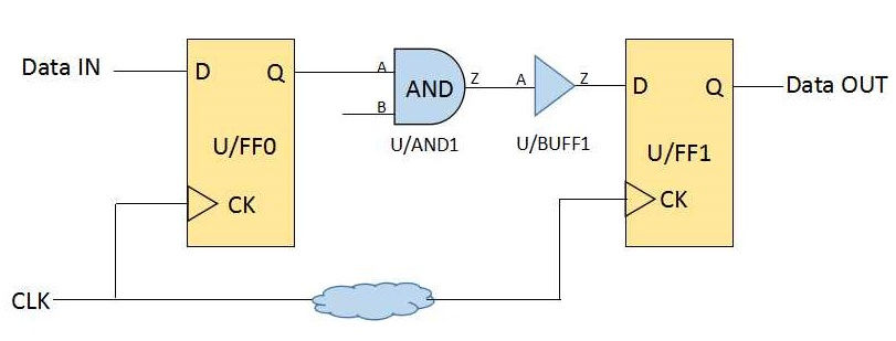
For analyzing the timing report, we will consider the R to R path in this blog. For other types of paths, the analysis and equations remain the same. Consider a path for analysis as shown in figure 1 and the timing report for the same path shown below it.
Setup Timing Report Analysis


Here, the clock network is considered as ideal for the sake of simplicity. The clock period is considered of 1ns. All other timings indicated in the report are in nanosecond (ns). Let us divide the timing report into 3 sections which are the top section, the middle section, and the bottom section. Now, let us understand each section in detail.
The first two lines in the top section of the timing report indicate the start point and the endpoint. Here, we have considered a reg to reg path so the start point and the endpoint both are rising edge-triggered flip-flops. Both the flops are clocked by a common clock CLK_A. For an inter clock path, there can be a separate clock for the launch flop and the capture flop. The path group in the third line indicates the clock by which the capture flop is clocked. In our example it is CLK_A. The next line gives information about the path type. As we are doing setup time check path type will be max. This suggests that the delays considered for the cells and the data path are maximum. These delays can be obtained either from the lib file or form the back annotated SDF file. In our example, we assume that the delays are taken from the lib file. In case of the delay obtained from the SDF file, a symbol of "&" is displayed along with the cell delay in the "Incr" column. In a similar way, minimum delays will be considered for the hold timing check.
The middle section represents the data path and the launch and the capture clock path. As we are considering an ideal clock network, the delay of the launch clock path will be 0.00ns as indicated in the report. Then the report shows the delay of each cell in the data path and wire delay as well. For example, delay 0.032ns corresponding to U/AND/A shows the time taken by data to travel from the Q pin of flop U/FF0 to the input pin A of gate U/AND. Whereas, the delay 0.12ns corresponding to U/AND/Z in the above report is the cell delay of the gate U/AND. The first column in the middle section represents the clock and pin names. The second column represents the incremental delay of each cell and the data path delay between two cells. The third column is for the cumulative delay of the path. There can be many other columns in the timing report such as the column for transition time, capacitive load, fanout load, etc. These columns can be printed by specifying the corresponding command arguments while generating the timing report. In the last column, "r" indicates the rising edge of the signal while "f" indicates the falling edge of the signal. Finally, data arrival time is the addition of all the delays in the "Incr" column and it is indicated in the last row of the "Path" column. The second half in the middle section is for the capture clock path. As setup time at the capture flop is always measured at the second clock cycle, the capture clock path begins from the delay equal to the clock period. In our example, the clock period is 1ns so the capture clock path will begin from the delay of 1ns. Other clock path delays are ignored as it is an ideal clock path. For the setup analysis, clock uncertainty will be subtracted from the clock period making the constraint tighter. Also, library setup time for the capture flop (U/FF1 in our example) will be subtracted from the clock period. This calculation gives the data required time for the capture flop. From the above report, the data required time is 0.70ns which means data should be stable at the D pin of U/FF1 on or before 0.70ns. If it fails so then the data will not be captured by the capture flip-flop. Here, also observe how clock uncertainty and the library setup time of the capture flop reduces our data required time.
The last and the bottom section of the timing report calculates the slack for the path. For setup time, slack is the subtraction of the data arrival time from the data required time. If slack is positive that means the path has met the setup timing requirement. Negative slack means the violation of the setup timing requirement. In our example, slack is 0.255ns indicating that the path under analysis will operate perfectly at the given frequency. In case if setup timing requirement does not meet even after trying all the possibilities, we can increase the frequency of the design to make the chip functioning properly.
Hold Timing Report Analysis
Let us consider the same figure 1 for the hold timing analysis. The hold timing report will be as below.
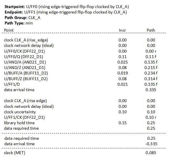
The top section in the hold report is the same as the setup timing report only the change is in path type. Here, the path type is "min" indicating the shortest path or the minimum delay considered for the cells and the data path during analysis. The middle section consists of the clock path delay and the data path delay. As the hold timing is measured at the same clock edge, clock delay at the capture side will remain 0ns instead of 1ns as in the setup timing report. Also, observe that the cell delay and path delay in this report is lower than that of the setup timing report. It is because for the best-case hold timing analysis we have to consider the shortest delay for the path. Here also the clock network delay is considered zero due to an ideal clock network. Unlike the setup timing report, here we have to add the clock uncertainty and the library hold time of the capture flop in the data required time. Finally, the third section shows the slack calculation. For hold timing report, slack is the subtraction of the data required time from the data arrival time. But in the timing report, it is shown as the required time minus the arrival time which will result in a negative slack. Thus, for hold timing report, a negative value of slack will be translated into a positive value which means the hold requirement is met while a positive slack value will be translated into a negative value indicating the hold violation.
In both the timing reports, near to the pin name, the library cell name is mentioned in braces. For example for AND gate, it is written like AND21_D1. Here, AND21 means it is a two-input AND gate with one output pin while D1 indicates the drive strength of 1. Similarly for other cells. The cell library is provided by the foundry so the naming convention may change from foundry to foundry or it can even change from one technology node to the another for the same foundry.
The main observations from this post are that we always perform the worst-case analysis for setup analysis. We do so in order to make sure that the chip will not violate setup timing even with the worst delay. For hold analysis, we consider the best-case analysis to ensure that hold timing will not violate even if the data transfer at the maximum possible speed.
In this blog, the analysis of the setup and hold timing report is covered. Here we have considered an ideal clock network and also the PVT (Process, Voltage, and Temperature) effects are not considered. Both the timing reports will become more pessimistic taking into account these effects. Regarding PVT analysis will discuss in a separate blog.
To read other blogs on physical design concepts click on the below links.
Please feel free to provide feedback on the information provided in this blog. To remain updated with the latest blog, subscribe to the website.
Thank You!
Stay Happy, stay safe...!! :)


Comments