
Setup and Hold Time - Part 1: The Introduction
- saumil vora

- Aug 5, 2020
- 6 min read
Updated: Aug 7, 2020
Greetings Readers!
After introducing the concept of STA in the previous blog (click here to read), now is the time to discuss one of the most important concepts of STA viz. Setup and Hold Timing analysis. The objective of this blog is to introduce setup and hold time, then we will discuss why it is required to check the setup and hold time. Let's begin with the definitions.
Defining Setup and Hold Time
Setup Time is the minimum amount of time before an active edge of the clock for which data should remain stable at the input pin of the register.
Hold Time is the minimum amount of time after an active clock edge during which data should remain stable at the input pin o the register.
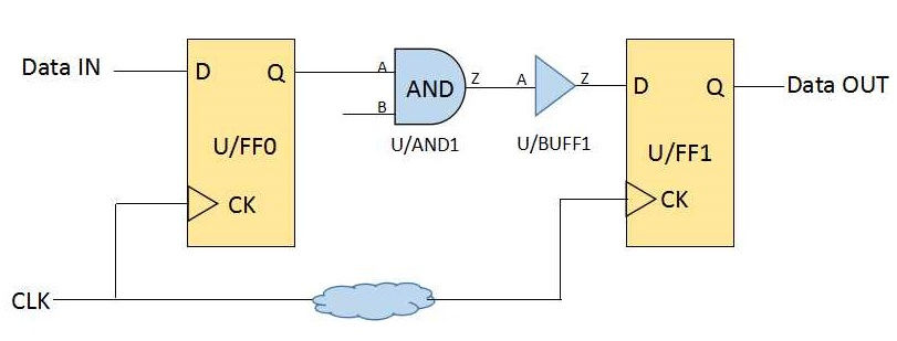

Consider a logic path under analysis as shown in figure 1. Here flip-flop U/FF0 is the launch flop and U/FF1 is the capture flop. Both the flip-flops are positive edge triggered. Let us consider a clock period as shown in figure 2. Let us understand the setup and hold time definitions w.r.t the capture flop (U/FF1).
At 0ps data will be launched from launch flop and let us assume that it takes 700ps to reach data at the D pin of flop U/FF1. Let us assume that the setup time for flop U/FF1 is 100ps (this information can be obtained from the lib file). This means data at the D pin of U/FF1 should remain stable for at least 100ps before an active edge of the clock. From figure 2 it is clear that the next active clock edge will occur at 1ns hence data should arrive at the D pin of U/FF1on or before 900ps. If data arrives after 900ps then it will not be captured properly by the capture flop and will fail the operation. This is called the setup timing violation. In our example data is arriving well before 900ps hence setup timing will not violate in this case. Hence we can say that data required time (1ns-100ps = 900ps) should be greater than the data arrival time (700ps). This difference is called slack. A positive slack means no setup violation in the design. The setup check is always done w.r.t the next clock cycle.
slack = data require time - data arrival time
data require time = clock period - setup time of capture flop (1ns - 100ps = 900ps)
data arrival time = CK->Q delay of launch flop + Combinational path delay (700ps)
Let us consider the hold time for flop U/FF1 in the library is 80ps. This means, after the active clock edge at 1ns, new data should not arrive at the D pin of U/FF1 for another 80ps. In our example data is taking 700ps to reach the D pin of U/FF1, hence hold time is also passing for our design. This makes the slack equation as below. Here also, positive slack means the design is free from the hold timing violations. The hold check is always carried out w.r.t the same clock cycle.
slack = data arrival time - data require time
data arrival time = CK->Q delay of launch flop + Combinational path delay (700ps)
data require time = library hold time for flip-flop
As the purpose of the setup timing check is to make sure that data should reach the input pin of the register prior to the clock edge, the purpose to check hold timing is to make sure that no new data should arrive at the input pin of the register until data is getting captured. Let us now explore why setup and hold time check requirement came into the picture.
Setup and Hold Time Equations
To derive the equations of setup and hold timing consider figures 1 and 2 shown above. Here register U/FF0 is the launch flop while U/FF1 is the capture flop. At the first rising clock edge, data will be available at the output of the register U/FF0. Then it traverses the combinational path and reaches the D pin of U/FF1. Data should become stable at the input of register U/FF1prior to the second active clock edge. This gives us the setup time equation as below.
setup time slack = (T_clk - Tsetup of the capture flop) - (Tck->q of launch flop + T_comb)
T_clk is the clock period
T_comb is the combinational path delay
In order to avoid setup timing violations, the below condition should be satisfied.
T_clk - Tsetup of capture flop >= Tck->q of launch flop + T_comb
data required time >= data arrival time
If we consider the clock uncertainty in calculation then the condition to satisfy the setup timing becomes as below. It further reduces the data required time and makes setup timing constraint tighter.
T_clk - Tsetup of capture flop - T_uncertainty >= Tck->q of launch flop + T_comb
If we consider a positive clock skew which eases the setup timing requirement then the equation becomes as below.
T_clk - Tsetup of capture flop - T_uncertainty >= Tck->q of launch flop + T_comb - Tskew
In the same way, from the hold time definition, the hold equation can be derived as below.
hold time slack = (Tck->q of launch flop + Tcomb) - Hold time of the capture flop
The below condition must be satisfied in order to meet the hold time requirement.
(Tck->q of launch flop + T_comb) >= Hold time of the capture flop
data arrival time >= data required time
Considering the clock uncertainty can further tighten the hold time requirements, the equation can be represented as below.
(Tck->q of launch flop + T_comb - T_uncertianity) >= Hold time of the capture flop
There is also the effect of skew on the hold time equation. A positive skew can further worsen the hold time constraints while a negative skew can ease it.
From Where Setup and Hold Time Comes?
Consider the figure 3 in which a D flip-flop is realized using two multiplexers. Further breaking down the design we get the transistor level structure as shown in figure 4.


Figure 3 and 4 represents a positive edge-triggered D flip-flop. As we already know that a D flip-flop is nothing but two back to back latches. Figure 4 shows the master and slave latches realized using pass transistors and inverters. As this is a positive edge-triggered flip-flop, data should be stable at the input of TR4 prior to the rising edge of the clock. Thus, we can say that the setup time is nothing but the time data takes to traverse the path I1-TR1-I3-I4 i.e. the delay of three inverters and one pass transistor. Initially, when the clock is a logic 0, pass transistor TR1 and TR3 becomes transparent. Data from D pin traverses the path I1-TR1-I3-I4. When the first rising edge occurs, pass transistors TR2 and TR4 becomes o transparent to the data while input pin D is isolated from the circuit. At this moment data is latched by the pass transistor TR2 and is available at the output pin Q through the pass transistor TR4 and inverter I6.
Similarly, the hold time is nothing but the time taken by the clock signal to reach the pass transistors in the master latch. Here for the sake of simplicity, the internal clock path is shown without inverters/buffers. There is a time difference between the arrival of the clock signal at the clock pin of the flip-flop and arrival of the same clock signal at the pass transistors inside. For example, a positive edge is occurring at 1ns at the CK pin of the flip-flop but it takes 200ps to reach the pass transistors. Thus, transmission gates TR1 will be turned off at 1.2ns instead of 1ns. This is the reason why new data should not arrive in this time frame otherwise chip will lose its functionality or can enter into a metastable state.
Sometimes we see a negative setup and hold time value for the flop in the timing library. The reason for negative library setup time for a flip-flop is that the internal clock path delay is greater than the internal combinational path delay (consisting of inverters and pass transistors).
setup time of flip-flop = internal cell delay - internal clock path delay
In the same manner, the reason for the negative library hold time for a flip-flop is that the internal combinational path delay (consisting of inverters and pass transistors) is greater than that of the internal clock path delay.
hold time of flip-flop = internal clock path delay - internal cell delay
In this blog, we have mainly discussed the basics of setup and hold timing. In upcoming blogs on STA, analyzing the setup and hold paths/reports will be discussed, stay tuned for that.
You can read blogs on other topics of physical design using the below links.
Please feel free to provide your feedback on this blog and please subscribe to stay updated for the latest post.
Stay Happy, Stay Safe... :)

Comments